- 您现在的位置:买卖IC网 > Sheet目录1991 > CS5346-CQZR (Cirrus Logic Inc)IC ADC AUD 103DB 200KHZ 48-LQFP
24
DS861PP3
CS5346
dress and set the read/write bit (R/W) high. The next falling edge of CCLK will clock out the MSB of the
addressed register (CDOUT will leave the high-impedance state).
For both read and write cycles, the memory address pointer will automatically increment following each
data byte in order to facilitate block reads and writes of successive registers.
5.7.2
IC Mode
In IC Mode, SDA is a bidirectional data line. Data is clocked into and out of the part by the clock, SCL.
There is no CS pin. Pins AD0 and AD1 form the two least-significant bits of the chip address and should
be connected through a resistor to VLC or DGND as desired. The state of the pins is sensed while the
CS5346 is being reset.
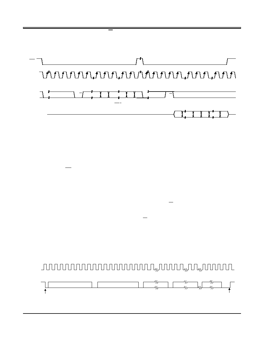
The signal timings for a read and write cycle are shown in Figure 15 and Figure 16. A Start condition is
defined as a falling transition of SDA while the clock is high. A Stop condition is a rising transition while
the clock is high. All other transitions of SDA occur while the clock is low. The first byte sent to the CS5346
after a Start condition consists of a 7-bit chip address field and a R/W bit (high for a read, low for a write).
The upper 5 bits of the 7-bit address field are fixed at 10011. To communicate with a CS5346, the chip
address field, which is the first byte sent to the CS5346, should match 10011 followed by the settings of
the AD1 and AD0. The 8th bit of the address is the R/W bit. If the operation is a write, the next byte is the
Memory Address Pointer (MAP) which selects the register to be read or written. If the operation is a read,
the contents of the register pointed to by the MAP will be output. Following each data byte, the memory
address pointer will automatically increment to facilitate block reads and writes of successive registers.
Each byte is separated by an acknowledge bit. The ACK bit is output from the CS5346 after each input
byte is read, and is input to the CS5346 from the microcontroller after each transmitted byte.
MA P
MSB
LSB
DATA
by te 1
by te n
R/W
AD D R ES S
CH IP
ADDRESS
CHIP
CD IN
CC L K
CS
CD OU T
MSB
LSB MSB
LSB
1001111
MAP = Memory Address Pointer, 8 bits, MSB first
High Impedance
Figure 14. Control Port Timing in SPI Mode
4
5
6
7
24 25
SCL
CHIP ADDRESS (WRITE)
MAP BYTE
DATA
DATA +1
START
ACK
STOP
ACK
1
0 0 1 1 AD1 AD0 0
SDA
6 6
5 4
3
2 1 0
7
6
1 0
7
6
1 0
7 6
1 0
0
1
2
3
8
9
12
16 17 18 19
10 11
13 14 15
27 28
26
DATA +n
Figure 15. Control Port Timing, IC Write
发布紧急采购,3分钟左右您将得到回复。
相关PDF资料
CS5351-BZZ
IC ADC AUD 108DB 204KHZ 24-TSSOP
CS5361-DZZ
IC ADC AUD 114DB 204KHZ 24-TSSOP
CS5364-CQZR
IC ADC 4CH 114DB 216KHZ 48-LQFP
CS5366-DQZR
IC ADC 6CH 114DB 216KHZ 48-LQFP
CS5368-DQZ
IC ADC 8CH 114DB 216KHZ 48-LQFP
CS5381-KSZ
IC ADC AUD 120DB 192KHZ 24-SOIC
CS53L21-CNZR
IC ADC STEREO 24BIT 98DB 32-QFN
CS5509-ASZR
IC ADC 16BIT SGL SUPP 16-SOIC
相关代理商/技术参数
CS5346-DQZ
功能描述:模数转换器 - ADC 103dB 24Bit 192kHz Stereo Audio ADC RoHS:否 制造商:Texas Instruments 通道数量:2 结构:Sigma-Delta 转换速率:125 SPs to 8 KSPs 分辨率:24 bit 输入类型:Differential 信噪比:107 dB 接口类型:SPI 工作电源电压:1.7 V to 3.6 V, 2.7 V to 5.25 V 最大工作温度:+ 85 C 安装风格:SMD/SMT 封装 / 箱体:VQFN-32
CS5346-DQZR
功能描述:音频数/模转换器 IC 103dB 24Bit 192kHz Stereo Audio ADC RoHS:否 制造商:Texas Instruments 转换器数量: 分辨率:16 bit 接口类型:I2S, UBS 转换速率: 信噪比:98 dB 工作电源电压:5 V DAC 输出端数量:2 工作温度范围:- 25 C to + 85 C 电源电流:23 mA 安装风格:SMD/SMT 封装 / 箱体:TQFP-32 封装:Reel
CS5349-000
制造商:TE Connectivity 功能描述:4110-10-340812
CS5349-BP
制造商:未知厂家 制造商全称:未知厂家 功能描述:Analog-to-Digital Converter, 16-Bit
CS5349-BS
制造商:未知厂家 制造商全称:未知厂家 功能描述:Analog-to-Digital Converter, 16-Bit
CS5349-KP
制造商:未知厂家 制造商全称:未知厂家 功能描述:Analog-to-Digital Converter, 16-Bit
CS5349-KS
制造商:未知厂家 制造商全称:未知厂家 功能描述:Analog-to-Digital Converter, 16-Bit
CS5351
制造商:CIRRUS 制造商全称:Cirrus Logic 功能描述:108 dB, 192 kHz, Multi-Bit Audio A/D Converter